

Samsung to Use TSMC's 3nm Process for Nvidia's Custom HBM Base Dies
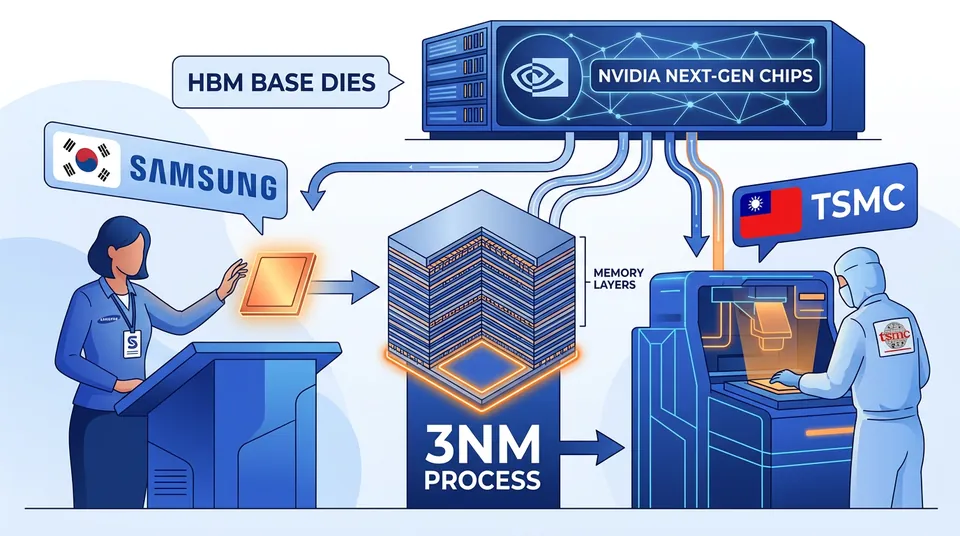
In a significant shift, Samsung Electronics will outsource a key component of its high-bandwidth memory for the first time, following a requirement from its major client, Nvidia. This move highlights the technical lead of rival TSMC in advanced manufacturing and a broader industry trend toward specialized production.
TechInsights estimates TSMC's N3 process yield is above 90%, while Samsung's comparable SF2 process yield is estimated to be between 50% and 60%.5
The global market for High Bandwidth Memory (HBM) is forecast by Counterpoint Research to reach approximately $100 billion by the year 2028.5
Nvidia's proprietary NVHBM architecture can increase memory bandwidth by up to 30% and reduce power consumption by 15% compared to the JEDEC HBM4E standard.5
Story
Nvidia's Mandate Reshapes Samsung's HBM StrategyAt the request of Nvidia, Samsung Electronics will utilize TSMC's 3-nanometer manufacturing process to produce the base die for Nvidia's next generation of custom high-bandwidth memory (HBM).1 This marks the first instance of Samsung collaborating with TSMC during the HBM manufacturing phase.1 The decision represents a departure from Samsung's established one-stop internal production model, where both the core memory and base logic dies were fabricated entirely on its own production lines.2 This strategic change was prompted by specific technical demands from Nvidia for its upcoming products.13
The primary driver for this shift is Nvidia's new NVHBM architecture, which was officially announced on August 26, 2026.15 This framework standardizes the memory system by integrating a custom memory controller directly into the base die.1 Nvidia has directed its three main HBM suppliers—Samsung, SK Hynix, and Micron—to use TSMC's manufacturing process for all NVHBM base dies to ensure uniformity.1 The core memory dies stacked on top of this base will continue to use sixth-generation DRAM technology.1
Samsung consented to Nvidia's requirement after completing an internal review of its own manufacturing capabilities.13 This internal assessment determined that the production yield of Samsung's own SF2 process could not meet the scale and reliability levels demanded by Nvidia.5 The substantial gap in advanced logic process yields between Samsung and TSMC is considered a key reason for Samsung's move to outsource the NVHBM base die.2 Estimates from TechInsights suggest Samsung's SF2 process yield is between 50% and 60%, while TSMC's N3 process yield is reported to be higher than 90%.5
This change in strategy is specifically for Nvidia's custom NVHBM orders.1 Samsung plans to continue its integrated, in-house manufacturing approach for standard HBM products and for orders from its other customers.1 The company is also assessing a contingency plan to use its own foundry division to produce the NVHBM base dies.14 This backup option would be considered if demand for the component surpasses TSMC's available production capacity, according to unnamed sources cited by the Seoul Economic Daily.4
Samsung's decision aligns with a broader trend seen among major HBM producers.1 Competitor SK Hynix, for example, had manufactured its base dies internally for all products leading up to HBM3E.1 However, upon advancing to the HBM4 generation, SK Hynix also transitioned to using TSMC's logic foundry services for its base dies.1 This shift by multiple top-tier memory makers indicates a growing reliance on specialized foundries for the advanced logic components required in next-generation HBM.1
These strategic moves are taking place within a rapidly expanding market for high-performance memory.5 Data from Counterpoint Research projects that the global HBM market will reach a value of approximately $100 billion by 2028.5 As of the middle of 2026, SK Hynix was the market leader, holding a share of about 50%.5 Nvidia's NVHBM initiative, by mandating a single foundry for the base die, aims to create a more consistent and interchangeable supply from its key memory partners.1
Nvidia's proprietary NVHBM architecture provides significant technical benefits when compared to the JEDEC HBM4E industry standard.5 It can deliver an increase in memory bandwidth of up to 30% per stack and reduce power consumption by 15%.5 The design also enables a reduction of up to 25% in the die area needed on the accelerator chip itself.5 By integrating the physical layer interface into the 3D stack, NVHBM reduces the area for the PHY and its supporting circuits on the accelerator by as much as 67% relative to the HBM4E standard.5
Concurrently with these strategic shifts in its memory business, Samsung is making substantial investments in its U.S. semiconductor manufacturing base.7 The company has pledged more than $22.8 million for workforce development and community programs in Central Texas.7 In 2025, Samsung's Austin and Taylor campuses are projected to inject $10.9 billion into the Central Texas economy.7 This economic activity is expected to support 28,746 jobs and generate $2 billion in local wages.7
Samsung's American expansion includes breaking ground in November for a second fabrication plant in Taylor, Texas.7 This new facility will span approximately 2.7 million square feet, with a target for mass production to begin in 2030.7 These investments are being made as the U.S. semiconductor industry anticipates a significant labor deficit.7 The industry group SEMI has estimated that the sector could face a shortage of up to 157,000 workers by the year 2030.7
TSMC, Samsung's partner and rival in this arrangement, is also expanding its manufacturing presence in the United States.7 The company's second fab in Arizona, which was recently completed, is scheduled to start mass production in the third quarter of 2027.7 TSMC CEO C.C. Wei also confirmed that the company has sent a team to assess Texas as a potential site for another factory.7 These parallel expansions highlight the intensifying investment and competition between the world's leading chipmakers on American soil.7
While navigating these complex changes in its core semiconductor business, Samsung continues to pursue ventures in other technology areas.6 For example, leaked specifications for a potential Samsung smart glasses device suggest it will use a Snapdragon AR1 Gen 1 chip.6 The specifications describe a device weighing 41 grams and equipped with 2GB of memory and 64GB of storage.6 This illustrates the company's continued diversification into consumer electronics alongside its strategic maneuvering in the foundry and memory markets.6
Structure
Who is connected to whom- 1Samsung Electronics
- ← competes withFact
- part of →Fact
- partners with →Fact
- supplies →Fact
- manufactures →Fact
Disagreements
Where the sources do not matchDate of Nvidia's NVHBM architecture announcement
科技新報1
techtimes.com5
Possibly: The sources provide different levels of detail for the announcement date. One gives only the month, while the other provides a specific day and year.
History
How it came to this- August 26, 2026Nvidia announces NVHBM architectureNvidia unveils its NVHBM framework, which integrates a custom memory controller into the base die to standardize the approach across different memory suppliers.
- October 18Samsung agrees to use TSMC processA report from South Korea's Seoul Economic Daily states that Samsung, after an internal review, has accepted Nvidia's requirement to use TSMC's 3-nanometer process for the custom HBM base dies.
- NowTSMC 3nm Samsung's process for Nvidia's custom HBM base die
- NovemberSamsung is expected to break ground on its second fabrication plant in Taylor, Texas. The facility, targeted for mass production in 2030, will expand Samsung's future foundry capacity.
Impact
Spreading outward, level by level- Level 1Samsung's HBM Production
For the first time, Samsung will collaborate with an external foundry, TSMC, for a stage of its HBM manufacturing. This move away from its one-stop internal production model is specific to Nvidia's custom NVHBM; Samsung intends to maintain its in-house method for standard HBM and other clients.12
Fact - Level 2Nvidia's Supply Chain
Nvidia has directed its key HBM suppliers—Samsung, SK Hynix, and Micron—to all use TSMC's process for the NVHBM base die. This standardizes a critical component, ensuring uniformity and interchangeability for its next-generation products.1
Fact - Level 3Broader Industry
Samsung's decision follows a similar move by competitor SK Hynix, which also turned to TSMC for its HBM4 base dies. This suggests a wider trend of memory makers outsourcing the advanced logic component of HBM to specialized foundries.
Analysis - Level 4Foundry Competition
The move reinforces TSMC's lead in advanced process technology, as the decision was reportedly driven by a significant yield gap between its 3nm process and Samsung's. Samsung is evaluating using its own foundry as a backup if demand exceeds TSMC's capacity.
Analysis
Ahead
Checked automatically when due; the result goes to the track recordSamsung is expected to break ground on its second fabrication plant in Taylor, Texas. The facility, targeted for mass production in 2030, will expand Samsung's future foundry capacity.
TSMC's second fab in Arizona is scheduled to begin mass production, increasing the foundry's overall capacity, which is critical for fulfilling large-scale orders for advanced nodes.
The global HBM market is projected to reach a value of approximately $100 billion, heightening the strategic importance of high-volume production and supply chain control for leading-edge memory.
Sources
What each source supportsWritten by AI from the sources listed below: every fact was checked word for word against its source, and inference is marked apart. How we write